


Intel has released product details for its first true graphics processor.
Based on Intel’s Xe microarchitecture, the new general-purpose graphics processing unit (GPGPU) is code-named “Ponte Vecchio”, borrowing from the name of the oldest bridge in Florence.
As opposed to churning out mind-blowing frame rates in video games, Ponte Vecchio has been designed for AI training, HPC modelling, and simulation workloads. Its targeted use cases include data centres, AI development, and scientific research.
Ponte Vecchio will debut as a showcase product for Intel’s 7nm transistors. It features a number of new technologies including Foveros 3D packaging technology, which minimizes footprint by stacking components on top of one another, and embedded multi-die interconnect bridge, a technology that allows layers of components to communicate through the stack.
This isn’t Intel’s first venture into the dedicated graphics scene. Back in 2010, Intel dabbed into the graphics scene with the Larrabee microarchitecture. The project was ultimately shelved as it fell short of expectations. Much of the research product from developing Larrabee was carried over to Xeon Phi, a co-processor produced in limited quantities.
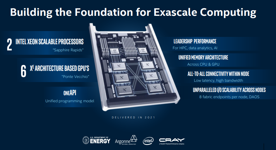
The Aurora system at Argonne National Laboratory will be the first U.S. exascale system to tap into Intel’s new hardware. It will feature two 10nm-based “Sapphire Rapids” Intel Xeon processors and six Ponte Vecchio GPUs. Aurora supports up to 10 petabytes of memory and 230 petabytes of storage. All the nodes will be connected using the Cray Slingshot interconnect, an ultra-high-speed network backbone that links together over 200 nodes.