


AMD’s third-generation Epyc processors, codenamed Milan, arrived on March 15 for cloud, datacentre, virtualization and high-performance computing (HPC) environments.
AMD Epyc 7003 lineup
There are 19 SKUs in AMD’s Epyc 7003 processor family. They range between eight to 64 cores, with two newly added 46 core and 56 core options. At the 32, 24, and 16 core levels, AMD segmented the product options to focus on either per-core performance, socket performance, or value.

Here’s how the lineup breaks down. The Epyc 75F3, 74F3, 73F3 and 73F2 are designed to push core performance for relational database and commercial high-performance compute use cases. The 7763, 7713, 7713P, 7663, and 7643 are optimized for core density, offering high core/thread count for maximum throughput per socket. The rest of the line from the 7313 to the 7543P provides a balance of performance and cost.
AMD also introduced the new 28-core Epyc 7453 to compete against Intel’s top-end Xeon processor. The company claims that it offers similar performance as its competitor at a lower cost.
All Epyc 7003 processors share a common feature set, including 8 channels of DDR4-3200 ECC memory support, 4TB of memory capacity, and 128 lanes of PCIe 4. As with the previous generation, Milan supports dual and single-socket configurations. Those that are single-socket only have the P suffix.
The third-generation Epyc processors are fully compatible with second-generation Epyc platforms. It’s a drop-in upgrade that requires only a BIOS update.

Architectural improvements
Milan uses AMD’s third-generation Zen architecture, the same as AMD’s consumer Ryzen 5000 series processors. Compared to Zen 2, Zen 3 has improved cache structure, better execution unit, and improved branch predictor. Milan also features a new die layout that reduced core-to-core latency and improved cache memory designs.


At the foundation of all Zen-based CPUs are Core Complex Dies (CCD). Each CCD includes eight cores. AMD connects multiple CCDs together over the Infinity Fabric interconnect to create chips with a higher core count. For example, the 16-core Ryzen 7 3800X has two fully-activated CCDs, while the 6-core Ryzen 5 3600X has two CCDs with 3 cores turned on for each.
Zen 3 solved one of Zen 2’s greatest issues: memory latency. In Zen 2, every CCD is further divided into two CCXs, or Core Cache Complexes. Each CCX had four cores and its own 16MB of L3 cache. However, this design introduced a latency penalty when cores on one CCX needed to access the cache on the other CCX. Zen 3 mitigated this issue by giving all eight cores a unified slice of 32MB L3 cache.
Moreover, Zen 3’s unified L3 cache structure provides more sources to the active cores in a low thread count workload, further reducing memory latency.

The shared L3 cache breaks down into shared data and per-core data. In Zen 2, the shared data section in one CCX needed to be duplicated onto the other CCX. It not only caused memory latency but also wasted die area. Zen 3’s unified L3 cache design gives all cores access to a single shared cache sector, freeing up more cache to store per-core data. Furthermore, even if just one core is enabled per CCD, it still can access the full cache pool without incurring a latency penalty.
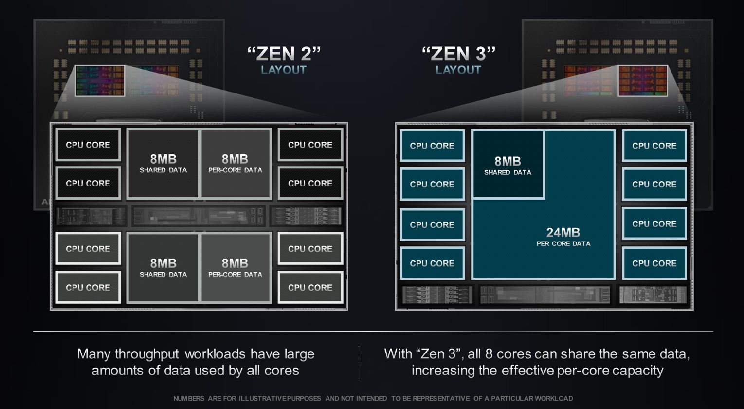
For SKUs with an odd number of cores, AMD simply disabled a core on every CCD.
All the inputs and outputs, including PCIe lanes and peripheral ports, are managed by the CPU without relying on a chipset. Upgrading from Rome to Milan is a drop-in process that only needs a BIOS update and does not incur any performance or feature penalties.
AMD explained that certain enterprise workloads frequently switch between the instruction and op-cache. Zen 3 has improved the performance of these workloads.
With an additional branch unit, Zen 3 increased the instruction window by 32, meaning it can have up to 32 more instructions in flight for out-of-order execution.
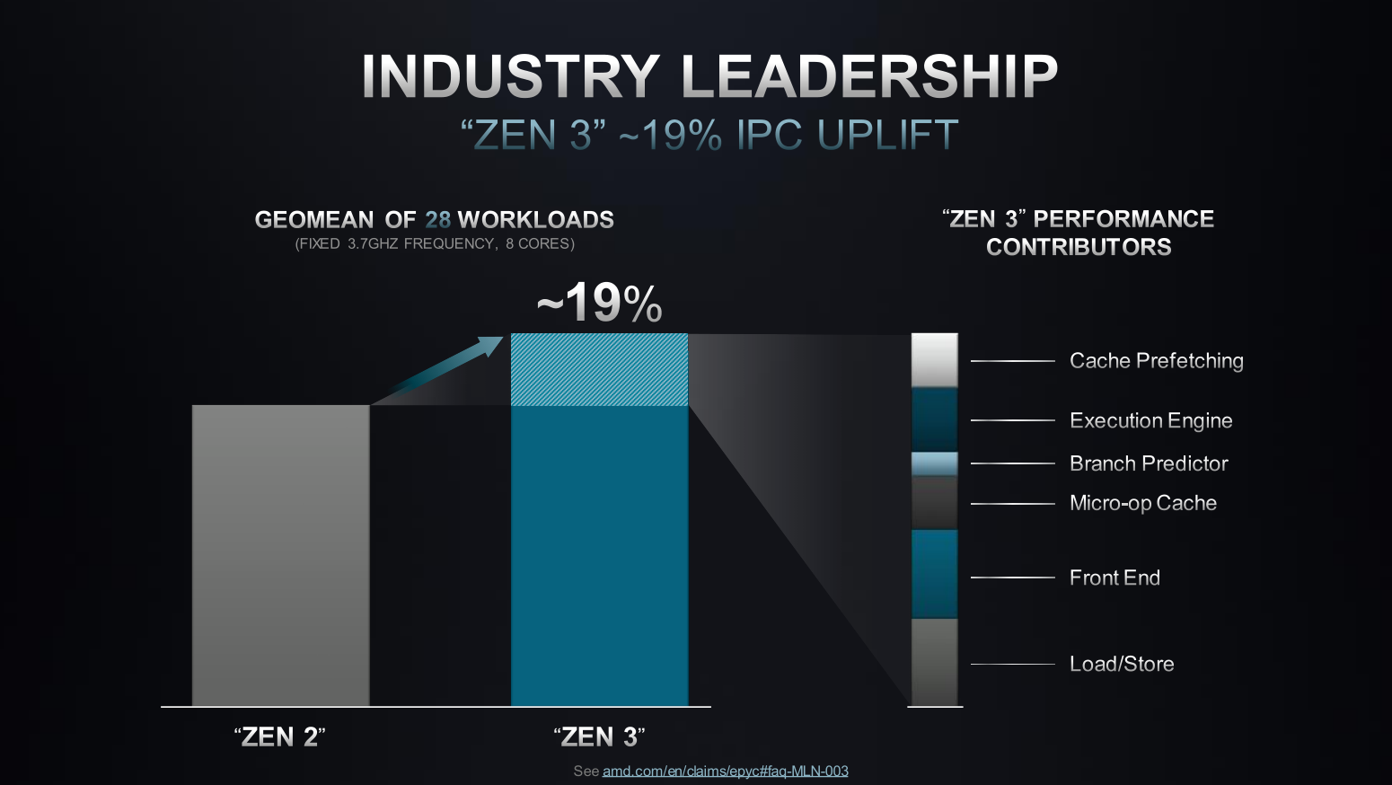
But not all instructions rely on floating points. Many AI inference workloads use lower precision integers. With Zen 3, AMD bolstered performance with int8, a common integer number size for AI inferencing, by doubling the floating-point pipelines from one to two to increase its throughput.
AMD also noted that Zen 3’s branch predictor is faster at recovering from a mispredict and is able to get to the correct instruction much faster.
Zen 3’s load/store unit can now do two stores per cycle instead of one. In addition, Zen 3 has four additional memory table walkers to increase random data performance when searching through large datasets.
Overall, AMD says that the Milan processors generally have double the performance of Intel’s Cascade Lake processors in HPC, cloud and enterprise workloads. AMD measured this using SPECate 2018 benchmarks.

AMD introduced two memory channel interleaving modes with Rome, allowing its customers to either populate the full eight memory channels for maximum bandwidth and capacity or only populate four for smaller-scale operations with lower memory performance requirements. Milan introduces a new six-channel mode to handle workloads that fall in between the two.
Security
Milan continues to use AMD’s Secure Processor, a tiny Arm-based co-processor embedded in the I/O die. Its functions include cryptography key generation and management, hardware-validated boot, and provide a hardware-based root of trust. Only the Secure Processor can access the keys.
These keys are used to encrypt DRAM. Memory can be encrypted using Secure Memory Encryption (SME), which encrypts the system memory with a key generated on each reset, or Secure Encrypted Virtualization, which generates a key for the hypervisor as well as a unique key for every guest to isolate the memory between guests as well as the hypervisor. Milan can support up to 509 simultaneous keys.
The AMD Secure Processor also performs hardware-validated boot and creates a hardware-based root of trust. During a boot sequence, the Secure Processor executes the on-chip boot ROM that loads and authenticates the off-chip bootloader, which sits in a section of flash memory on the socket. Once it verifies the off-chip bootloader, the Secure Processor switches from executing the on-chip boot ROM to executing the off-chip bootloader, followed by the bootloader providing the instructions needed to load other items, such as the key management’s OS and kernel, before loading the x86 BIOS.
Additionally, AMD hardened virtualization security by adding SEV-SNP, or Secure Encrypted Virtualization with Secure Nested Paging. SEV-SNP protects a guest operating system from an untrusted hypervisor by preventing writes to the guest’s virtual machine. It also defends against replay corruption or remapping attacks by a malicious hypervisor.